Quality Digest does not charge readers for its content. We believe that industry news is important for you to do your job, and Quality Digest supports businesses of all types.
Our PROMISE: Quality Digest only displays static ads that never overlay or cover up content. They never get in your way. They are there for you to read, or not.
Published: Wednesday, September 13, 2023 – 12:00
The system is designed with safety in mind; a protective cover is provided to prevent possible damage due to operator error. Operation meets SEMI international standards S2, S8, and F47.
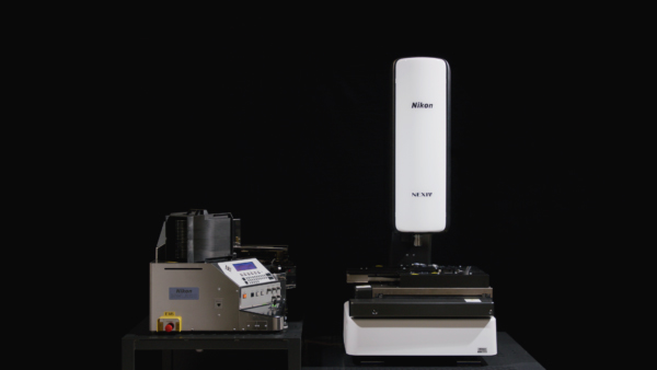
NEXIV VMZ-NWL 200 is a system that automatically measures 6-in. or 8-in. wafers held in a carrier according to a measurement program. High repeatability is ensured by the reliability of the NEXIV and stable wafer loading using the NWL. The system allows intuitive selection of the chip being measured using dedicated software. This way, anyone is able to achieve the chip measurement results they need with a high degree of reliability. In addition, it is possible to trace when the measurement was performed and by which program.
Thanks,
Quality Digest
منبع: https://www.qualitydigest.com/inside/innovation-news/wafer-automatic-measurement-solution-nikon-091323.html(Nikon Industrial Metrology: Brighton, MI) — The Industrial Metrology business unit of Nikon Corp. has released the automatic wafer measurement system NEXIV VMZ-NWL 200 to solve the challenges of wafer metrology in the semiconductor back-end process, where more work is traditionally carried out manually than in front-end process control. The main target market for NEXIV VMZ-NWL 200 is measurement, centered on semiconductor manufacturing processes in the back end.
However, someone has to pay for this content. And that’s where advertising comes in. Most people consider ads a nuisance, but they do serve a useful function besides allowing media companies to stay afloat. They keep you aware of new products and services relevant to your industry. All ads in Quality Digest apply directly to products and services that most of our readers need. You won’t see automobile or health supplement ads.
NEXIV VMZ-NWL 200 alleviates the shortage of skilled technicians for manual measurement. The semiconductor industry has developed along the path of miniaturization, which has increased the skill level required for measurement and reduced the number of available engineers. On the other hand, the semiconductor market continues to expand so the increasing metrology opportunities are being offered to ever fewer people. As a result, manual measurements using conventional optical microscopes have reached their limits.
So please consider turning off your ad blocker for our site.
Innovation
Wafer Automatic Measurement Solution from Nikon
Supports back-end process control